
Resources
Explore Datasheets, Videos, Technical Papers and More
Videos
Solstice® Single-Wafer Platform for Advanced Packaging
Solstice® Sizzle
Solstice® Solvent Processing / MLO Explainer video

Why Solstice® is the Choice of Compound Semiconductor Fabs
Solstice® Single-Wafer Platform:
Advanced Electroplating and Surface Prep
ClassOne’s Technology
Development Center
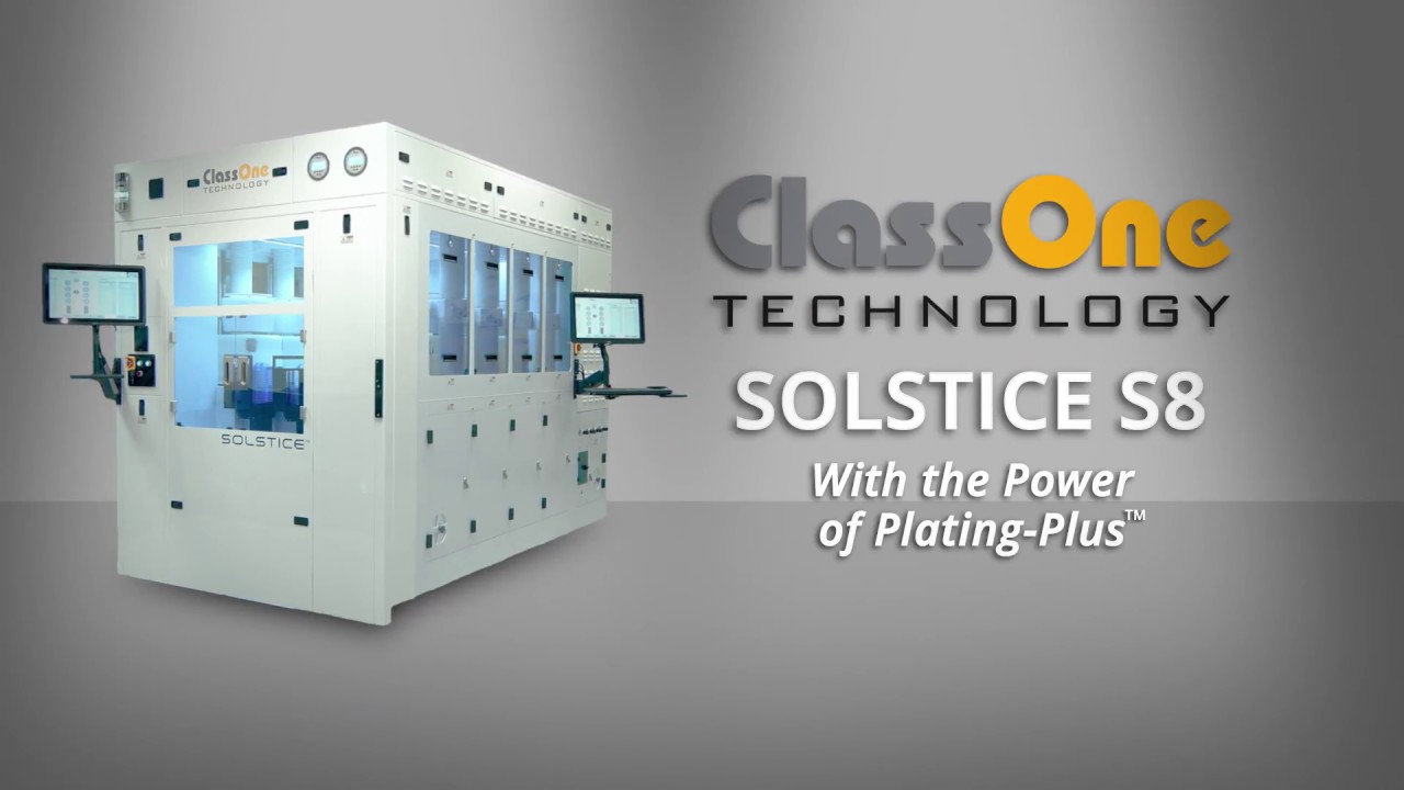
Solstice® S8 Automated Electroplating Overview

Setting Up Your New Electroplating Line
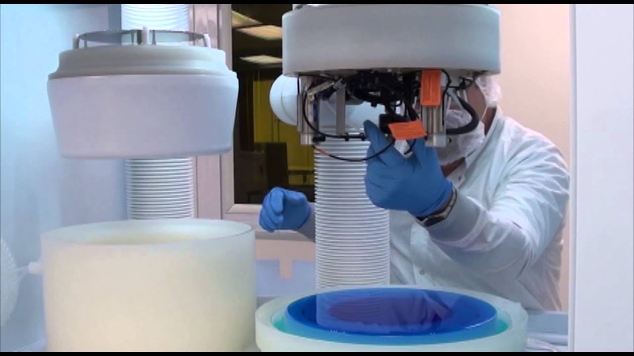
ClassOne Solstice® Fast Rotor Change
ClassOne Solstice® LT Electroplating Tool
Solstice® Electroplating with Plating-Plus™
Solstice® Single-Wafer Platform for Advanced Packaging
Solstice® Sizzle
Solstice® Solvent Processing / MLO Explainer video
Why Solstice® is the Choice of Compound Semiconductor Fabs
Solstice® Single-Wafer Platform:
Advanced Electroplating and Surface Prep
ClassOne’s Technology
Development Center
Solstice® S8 Automated Electroplating Overview
Setting Up Your New Electroplating Line
ClassOne Solstice® Fast Rotor Change
ClassOne Solstice® LT Electroplating Tool
Solstice® Electroplating with Plating-Plus™
Application Datasheets


Brochures & Product Datasheets


White Papers

Technology Papers
Advanced Semiconductor Plating – Key Fundamentals
Process Application Note #100 – This paper provides background fundamentals of electrochemical deposition (ECD) in the semiconductor industry for engineers, technicians, and other personnel involved in plating processes. See Summary Overview
Electroplating Fundamentals – Optimizing Cross-wafer
Process Application Note #101 – This paper presents the basic principles and methodologies for helping process engineers to achieve optimized cross-wafer uniformity in semiconductor electroplating. It provides guidance for users of different plating systems. See Summary Overview
Articles & Viewpoints


