Systems Designed for Advanced Microelectronics Markets

Specialized electroplating and wet processing technologies for advanced semiconductor and compound semiconductor manufacturing
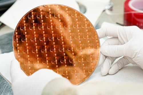
We all want to make a difference. You do it by building the devices that change and enhance the lives of people around the world – such as microLEDs, RF and power devices, advanced VCSELs and advanced sensors. We do it by providing you with the right tools for the job. Since 2013, we’ve provided you with the world’s most elegantly designed advanced electroplating and wet processing systems to take your innovations from the lab to the fab. Below are markets we specialize in.


Semiconductors


Volume manufacturing and innovative R&D

Semiconductor device proliferation is driven by pervasive demand in nearly every consumer product, from toothbrushes to automobiles. The modern world is dependent on reliable and cost-effective semiconductor devices that help collect, transmit, process, and store information.  For example, in a car, a MEMS sensor can collect pressure data from a tire. An Application Specific Integrated Circuit (ASIC) could be used to process the digital signal into useful data. A low-energy RF chip can forward the data to the main car computer. The main computer uses powerful memory and logic chips to analyze the data and potentially trigger an event. A solid-state storage chip then archives the data for future review or analysis. In every modern system that processes data, semiconductor devices are an irreplaceable component.

ClassOne’s Technology in Electroplating and Wet Process provides our customers the ability to create today’s and tomorrow’s semiconductor devices. The Solstice Platform flexibility and ClassOne’s partnership-focused culture provides solutions for volume manufacturing of legacy technology as well as innovative solutions for R&D pathfinding. 

VSCEL


A VCSEL featuring Solstice gold plating.

Exceptional VCSELs beam quality and application performance

VCSELs, or Vertical-Cavity Surface-Emitting Laser devices, are high-efficiency semiconductor laser diodes that emit a laser beam perpendicularly from the top surface, as opposed to the edge-emission of other semiconductor lasers.

Low-power VCSELs can provide superior beam quality, a symmetric beam profile, and low beam divergence, compared with edge-emitting laser diodes. This enables the VCSEL output beam to be collimated with a simple lens without a high numerical aperture. And because of its uniquely focused light, spectral purity and stable wavelength, VCSELs can provide extremely high performance and efficiency in numerous sensing applications.

VCSELs are used in many next-generation laser products, including 3D sensing, facial recognition, 2D imaging, smart-glasses, fiber optic communications, LIDAR and ranging, gas-sensing, and laser-based materials processing.

ClassOne has developed several proprietary high-performance wet-processing capabilities that are of special interest to VCSEL manufacturers who require high-speed, high-quality, cost-cutting plating – in particular, for gold, nickel, and copper.


Display


Higher brightness, lower power, longer life

advanced new devices

Electroplated gold plug used in microLED device.

As the name implies, microLEDs are “micro-sized” LEDs (light emitting diodes), measuring less than 100 µm in size. Like the traditional OLEDs (organic LEDs), MicroLEDs are “self-emitting,” so each red, green, and blue sub-pixel produces its own light – unlike LCDs, which require backlighting. But unlike organic LEDs, microLEDs are fabricated out of gallium nitride (GaN), which is inorganic and gives them much longer life.

MicroLEDs are enabling many new enhancements in display applications as well as photonics. In displays, microLEDs can deliver significantly higher brightness and contrast, ultra-low power consumption (for extended battery life), ultra-high resolution, no problem with off-angle viewing, fast response, high reliability, and long lifetime, among other advantages.

In addition to direct-view displays. microLEDs are also enabling very-high-density micro-displays for use in projectors, AR/VR, and head-up displays. MicroLEDs can enable flexible displays as well as many small, low-energy devices such as smart watches and smart phones.

While the micro size of microLEDs gives many advantages, it often necessitates using many thousands of devices for each end product. And this dramatically increases the need to maximize yields and maintain consistently high performance in the devices. These are just two of the areas in which Solstice and ClassOne are assisting industry-leading fabs in delivering the highest quality next-generation microLEDs.


MEMS and Sensors


Reliability, simplicity, flexibility

Advanced microelectromechanical systems (MEMS) and sensors are becoming key elements in today’s newest devices and vehicles and a rapidly-growing list of other commercial and industrial applications. For example, radar proximity sensing is applied in autonomous vehicles, ultrasonic-sensing for vehicle back-up assist, infrared sensors for many forms of remote control, and image sensors are incorporated in numerous camera and vision systems. In addition, there are IC temperature sensors, pressure sensors, shear stress sensors, on and on.

Combined via and RDL feature for probe card device.

Fabricating this wide array of sensing devices requires many leading-edge semiconductor processes. It also requires flexibility in the processing equipment, because the technologies and device configurations are constantly advancing and changing. For plating and surface preparation processes, ClassOne’s Solstice systems are often selected because they give manufacturers both advanced performance and maximum flexibility to address a broad range of needs. For example, Solstice can be used for multi-metal stacked plating of hermetically sealed boxes, pillars and solder bump, high-speed copper pillar and RDL deposition, and perfectly flat gold features for thermo-compression bonded pads and n- and p- contacts. In surface prep, Solstice enables metal lift-off, UBM etching, patterned metal etching, precision anodization, stress relief etching, substrate thinning, and more. All of that is made possible by one very flexible platform.


RF and Power Devices


Compact, low-cost, high-frequency, increased bandwidth

RF signal filtration is enabling tomorrow’s communications by eliminating noise and cleanly separating frequency bands. State-of-the-art SAW (Surface Acoustic Wave) and BAW (Bulk Acoustic Wave) filters are helping to achieve the goals of higher bandwidth, lower cost, and increasing device density for 4G and 5G mobile communications.

A BAW filter for 5G plated by ClassOne’s Solstice.

Both types of filters convert electrical energy into mechanical or acoustic energy and back again to an electrical signal; however, they differ in the architecture of the device. SAW filters produce acoustic waves within the surface of a piezoelectric substrate. This is accomplished by passing the
signal through a band of interlacing ‘comb’ structures which are fabricated on a single plane. BAW filters are constructed in multiple layers, with the wave being induced through the bulk of the piezoelectric substrate between an upper and a lower electrode.

SAW filters can provide advantages in their simplicity and generally lower cost. BAW filters can provide superior signal processing, especially at higher frequencies such as those associated with 5G signal processing requirements.

For both types of devices, the high demands on the newest wireless communication systems require increasingly advanced filter fabrication which calls for class-leading metal deposition at low CoO. Which is why ClassOne’s Solstice platform – and the GoldPro reactor specifically – are often the preferred choices for RF device manufacturers.


Advanced Packaging


Submicron Copper Via used in Hybrid Bonding

10×100 micron TSV filled on Solstice.

Advanced packaging and Heterogenous Integration, including Through-Silicon Via (TSV), hybrid bonding, and interposers are pivotal for enhancing integrated circuits in size, power, performance, and integration. TSVs enable vertical interconnects through the silicon substrate, reducing signal transmission delays and allowing for 3D stacking of chips. This technology improves overall IC performance through shorter interconnects, and aids in efficient heat dissipation.

Hybrid bonding involves atomic or molecular-level connections, often copper-to-copper, offering high-density, fine-pitch interconnects with superior electrical characteristics. Hybrid bonding excels in achieving low resistance and capacitance, accommodating various materials, and supporting versatile chip integration. Solstice’s capability to control uniformity and support in cutting edge chemistry control allow for manufacturers to improve yield and bonding integrity.

Solstice and ClassOne are serving industry and academia as these process integration technologies further develop. Solstice’s capability in plating control has been an integral part of the success of TSV, Hybrid Bonding and Interposer technologies. ClassOne is also very excited about supporting Packaging research centers as the next generation of Advanced Packaging is developed and commercialized.


© 2024 ClassOne Technology All rights reserved.
Click to access the login or register cheese