Indium Bump Plating
Using the Solstice® Gen4 Chamber
Enabling Indium Interconnects for Emerging Technologies
Indium has long been used in infrared imaging and detector applications, but growing investment in quantum computing, cryogenic electronics, advanced sensors, and space systems is driving renewed interest in indium-based interconnect technologies.
Unlike conventional solder materials, indium offers exceptional compliance, low-temperature bonding, and superconducting behavior at cryogenic temperatures, making it uniquely suited for applications where reliability and performance must be maintained under extreme operating conditions. Electroplated indium bumping provides a scalable approach for manufacturing the fine-pitch interconnects required by these next-generation devices.
Key Process Requirements
- Fine-pitch bump formation
- Uniform bump height
- Tight thickness control
- High process repeatability
- Production-ready throughput
Successfully meeting these requirements depends on both plating chemistry and reactor design.
Solstice® Indium Electroplating Utilizing the Gen4 Chamber
The Solstice® platform delivers the process flexibility required for advanced indium plating applications, including:
- Precision electric field control
- Flexible process recipe architecture
- Inert atmosphere reactor capability
- Integrated bath monitoring and control
- Rapid wafer transfer
- High-uniformity plating performance
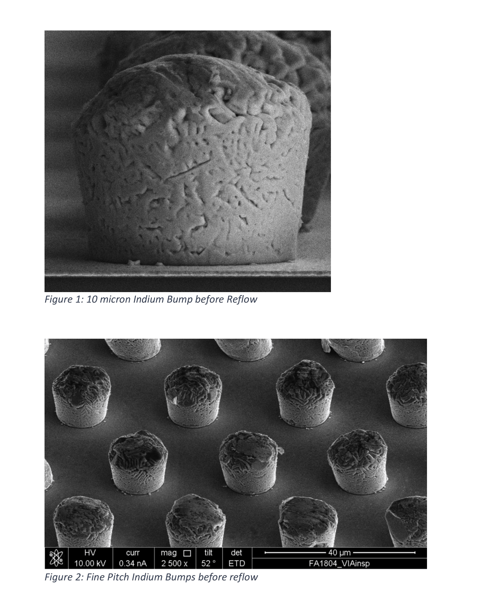
The result is reliable indium bump formation capable of supporting pitches down to 10 microns and beyond.
A Flexible Platform for Emerging Applications
Because indium bumping is often used in specialized and rapidly evolving applications, process flexibility is critical. The modular Solstice® platform enables customers to develop, optimize, and scale indium bump processes from R&D through production while maintaining process consistency and high throughput.
Resources: