Electroplating and Wet Processing for Advanced Microelectronics
Delivering Unmatched Performance and
Process Flexibility with Maximum ROI
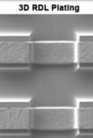
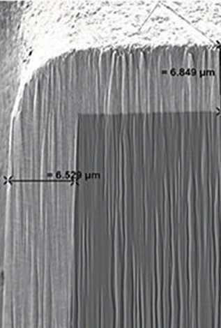
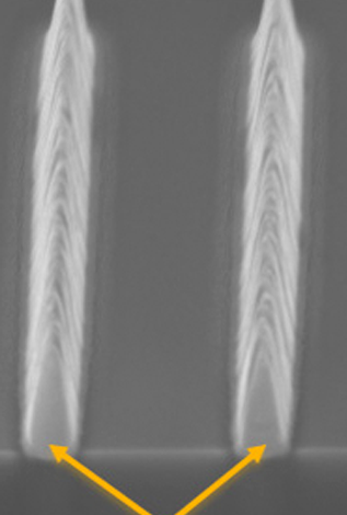
Advanced Packaging
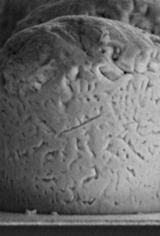
Advanced Gold Plating
Solvent Processing
Wet Etch and Cleans

Emerging Technologies
Top Process Applications
Solstice supports five core backend applications: Advanced Packaging, Advanced Gold Plating, Solvent Processing, Wet Etch and Cleans, and Emerging Technologies. Each application is powered by modular, high-performance chambers that deliver precision, flexibility, and simplicity for both production and R&D environments.
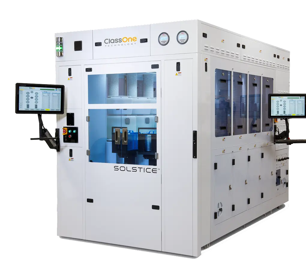
Solstice
The Solstice platform provides a common, easy to use, high performance flexible platform for many process technologies across Electroplating and Wet Process.
The Solstice Max and Solstice S platforms provide high performance process technologies for surface prep and electroplating. Solstice chambers seek to maximize performance to complexity + cost. In all the chamber technologies, unnecessary complexity common to competitors has been removed in favor of more elegant and intuitive designs. This allows for faster recipe dial in, longer up times, and lower burdens for operators and engineers.
Max Series
- Modular platform, extendible in the field
- 200mm and 300mm wafer capable
- From 2 to 16 chambers
S-Series
- Monolithic frame
- 3-inch to 200mm wafer capable
- From 2 to 8 chambers
- Smallest footprint

Visit us at SEMICON West!
October 13-15, 2026 | San Francisco, CA


