Hybrid Bonding
Using the Solstice® CopperMax™ and GoldPro™ Chamber
Enabling the Next Generation of Semiconductor Integration
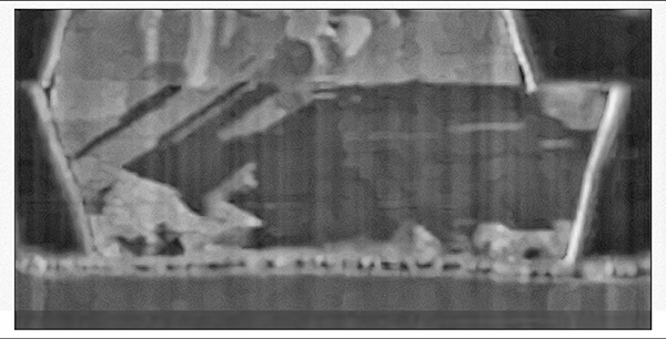
Hybrid bonding continues to be an end goal for advanced packaging, enabled by dense, uniform pillar and via structures. Coplanarity, metal grain orientation, and surface cleans can be successfully optimized using Solstice. ClassOne continues to work with select partners across the advanced packaging space to bring hybrid bonding technology to maturity.
As AI, photonics, memory, and advanced logic devices demand higher bandwidth, lower power consumption, and greater integration density, traditional interconnect technologies are reaching their limits. Hybrid bonding has emerged as a key technology for advanced packaging, enabling direct electrical and mechanical connections between wafers and chips at unprecedented densities.
By eliminating many of the limitations associated with micro-bumps and solder-based interconnects, hybrid bonding helps manufacturers achieve higher performance, lower power consumption, and smaller device footprints.
Through-Glass Via • Copper Pillar Plating • Multi Metal Stack Pillar
How ClassOne Enables Hybrid Bonding
Copper (Cu) remains the dominant metal used in advanced hybrid bonding architectures. The Solstice® CopperMax™ chamber delivers highly uniform copper deposition and feature filling across the wafer, helping manufacturers create the precise copper structures required for reliable Cu-to-Cu hybrid bonding.
For photonics, compound semiconductors, MEMS, RF, and specialty device applications, gold-based bonding architectures can provide important performance and reliability advantages.
The Solstice® GoldPro™ chamber delivers highly uniform, low-defect gold deposition for applications requiring advanced gold interconnect structures and bonding surfaces.
Advanced Wet Processing & Surface Preparation
Surface quality is critical to hybrid bonding success. Solstice® platforms integrate advanced cleaning, rinsing, and surface preparation capabilities designed to help customers achieve the cleanliness, coplanarity, and surface condition required for high-yield bonding processes.
Process Enablement for Advanced Packaging
ClassOne does not provide the bonding tool itself. Instead, ClassOne enables the critical plating and surface preparation processes that make hybrid bonding possible.
By delivering precise metal deposition and advanced wet processing on a common Solstice® platform, ClassOne helps customers develop and scale hybrid bonding process flows for advanced packaging, photonics, compound semiconductors, MEMS, and next-generation semiconductor devices.