
Gold Deplating
Using the Solstice® Gen4 ECD Chamber
Electrolytic gold deplating is a precision wet-processing technology used to selectively remove exposed gold seed layers after electroplating for feature isolation. The Solstice® platform delivers highly uniform, tightly controlled gold removal with minimal undercut, low surface roughness, and exceptional process repeatability. Compared to conventional dry etch methods, Solstice provides a lower-cost, higher-throughput solution that preserves critical feature dimensions while integrating plating, deplating, and surface preparation on a single automated platform.
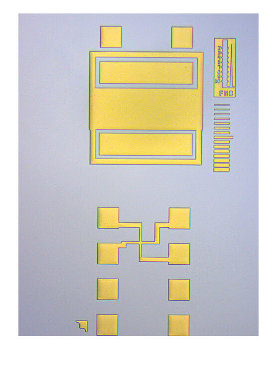
Our highly stable, cost-effective electrodeposition process is ideally suited for use in forming features such gold bond pads or gold bumps. A subsequent photoresist strip step is followed by the removal of the original gold seed, otherwise known as feature isolation.
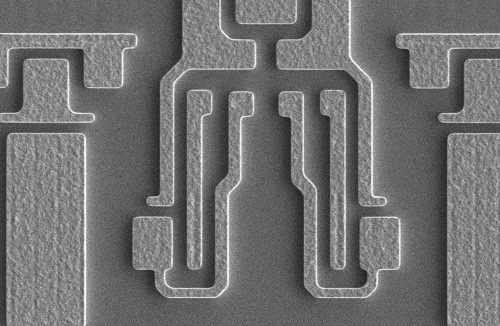
This feature isolation step can be performed using dry etch in a vacuum chamber, but that process is expensive and results in a roughened surface of the plated feature. Electrolytic gold deplate is a much lower-cost option that results in minimal CD loss and the smoothest possible gold surface. Further, the process step integrates easily into our advanced and flexible Solstice® plating tool when combined with our proprietary Gen4 ECD chamber.
Applications
- Bond pads for microLEDs
- VCSEL p- and n-contact plating
- Gold bump
- BAW and SAW filters
- Air-bridge
- And more…
Features
- Precision wafer rotation, closed loop flow control
- Voltage-controlled recipe construction
- Continuously filtered chemistry loop
- Optional carbon filtration
- Adjustable diffuser
- Wet-contact plating rotor, customized contact reach
- Levitronix® pump with LeviFlow™
Benefits
- Extremely uniform removal
- Optimal, responsive removal rate
- Extremely uniform field profile
- Contact reach aligns to existing integration
- Accurate, precise flow rate control
| Technical Data | |
| Wafer Materials | Silicon GaAs GaN on Si, GaN on Sapphire Sapphire Transparent substrates and more |
| Flow Rate | 30 lpm |
| Plating Rate | Up to 150μm/minute |
| Within-Wafer Uniformity | <3% (range 2*mean) |
| CD Reduction | <0 2Å on 1200Å seed deplate |
| Within-Wafer Uniformity | <2% |
| Within Feature Uniformity | <2% |
| Roughness | 3A Ra |


