
Patterned Gold Plating
Using the Solstice® GoldPro™ Chamber
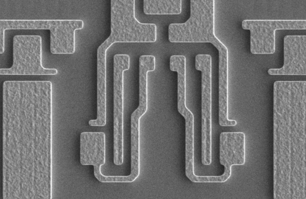
For RF and photonics devices, gold plating plays a vital role in device performance. You will find high-speed plating in a gold sulfite bath is sensitive to localized flow vectors due to the relatively slow diffusion rate of gold complex ions. As a result, a sub-optimal electrolyte flow profile results in a non-flat plated feature shape. To overcome this issue, most immersion and fountain plating systems require very low plating rates.
Our proprietary Solstice® GoldPro™ chamber generates randomized fluid vectors at the diffusion layer of the wafer. This ensures that the diffusion layer is as thin as practical, and that fluid motion remains directionless. Ultimately, this results in a flat plated feature profile without sacrificing plating rate.
Applications
- Bond pads for microLEDs
- VCSEL p- and n-contact plating
- Gold bump
- BAW and SAW filters
- Air-bridge
- And more…
Features
- Randomized fluid vectoring
- Adjustable diffuser
- Dissolved oxygen control
- Dry-contact, low maintenance plating rotor
- Customized seal reach
- Continuously filtered chemistry loop
- Optional carbon filtration
- Levitronix® pump with LeviFlow™
Benefits
- High plating rate and high uniformity
- Extremely uniform field profile
- Maximized bath life
- Seal reach aligns to existing integration
- Continuously cleaner chemistry
- Precise, consistent flow rate control
| Technical Data | |
| Wafer Materials | Silicon GaAs GaN on Si, GaN on Sapphire Sapphire Transparent substrates and more |
| Flow Rate | 30-60 lpm Dependant on wafer size |
| Plating Rate | Up to 1μm/minute (depend on chemistry) |
| Within-Wafer Uniformity | <2% |
| Within Feature Uniformity | <2% |
| Roughness | <2kA |