MARKET BRIEF: UNIVERSITY R&D SPOTLIGHT
From University to Industry: Bridging the Manufacturing Path
ClassOne Technology’s Solstice single-wafer platform is affording new opportunities for universities and research institutions to up their manufacturing game at an attractive cost
The university setting offers a valuable environment for future engineers to explore and learn about technologies that will become part of their daily lives when they transition from school to career. At the same time, universities that are working on microelectronics and advanced R&D are increasingly looking for more advanced manufacturing equipment that offers both reasonable upfront investment cost and a low cost of ownership.
Over the next five years, we will see major changes in the kinds of microelectronics projects and programs that universities pursue. University fabs are moving toward advanced fab-level wafer processing and away from the benchtop beakers and wet benches that were not equipped to deal with new and emerging challenges. With the passage of the U.S. CHIPS and Science Act, universities are looking to take a major leap forward in capability to more readily transfer technology to the chip manufacturing industry.
Engaging with advanced tools is also more interesting than working with wet benches, which will inspire students to join the industry and be better prepared to work in real fabs. This will be vital to filling the semiconductor industry’s need for skilled workers. According to a recent Semiconductor Industry Association (SIA) report, the workforce will grow to approximately 460,000 jobs by 2030, representing 33% growth from today’s 345,000 jobs. However, at the current rate of degree completion, 58% of these projected new jobs (and 80% of projected new technical jobs) may go unfilled.
Universities are thus under added pressure to attract and excite students to enter the industry by providing relevant curriculums and imparting real-world skills. Bringing more advanced tools to universities will also mirror what’s being used in the semiconductor industry – essentially setting up universities to become an adjunct for industry development.
Some university cleanrooms are already adding the kinds of production-proven, fully automated high-volume tools that are found in today’s semiconductor facilities. For other schools, while this level of investment is aspirational, they plan to have significant funds available to spend on their cleanroom setups and need an affordable, yet powerful, tool to help move them along the path toward industry-level offerings that allow them to optimize at-premium fab space.
The lab-to-fab solution
Many universities looking to offer more leading-edge capabilities are focusing on advanced packaging (AP). According to market research firm Yole Group, this industry’s market value is projected to grow from US$ 44.3 billion in 2022 to US$ 78 billion by 2028 – a 10% CAGR. AI and machine learning are enabling data center, automotive, 5G and other applications that require powerful processors to handle the sheer volume of data being generated. In turn, these devices necessitate use of AP techniques.
Electroplating is a key AP process, enabling fast, cost-effective formation of electrical features and metallic connections. This is creating a huge opportunity for ClassOne Technology, as demand for its Solsticeâ single-wafer processing platform by universities across North America is rapidly accelerating. The Solstice platform is uniquely suited to serve as the bridge tool from wet bench to single-wafer processing for universities, as well as research institutions. Specifically designed for electroplating and surface preparation processes, Solstice provides the ability to configure an AP cluster system, where plating, photoresist strip and wet etch are all performed on one tool with a highly compact footprint.
One example of the technologies that universities are researching is ultra-high-aspect-ratio through-silicon via (TSV) features on semiconductor wafers, for which Solstice Vacuum Pre-Wet and CopperMax chambers allow universities to continue pushing the aspect-ratio boundary. Additionally, universities are delving into new areas like quantum computing; here, Solstice is able to handle novel processes and unique materials in advanced applications, including indium and aluminum. Universities see Solstice as the solution for new process flows and ClassOne as a valuable partner.
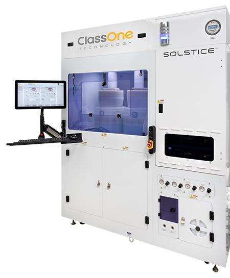
The Solstice LT single-wafer wet processing system from ClassOne Technology is in increasingly high demand from universities looking to make the lab-to-fab transition
Solstice is available in three primary models that can be configured in numerous ways to process virtually any type of wafer substrate from coupon to 200mm in diameter:
- LT, with up to three chambers, is a manual system ideally suited for low-volume/R&D using the same chamber architecture as the automated systems.
- S4, with four chambers suited to pilot production and robotic wafer handling, allows students the opportunity to gain experience in programming automation.
- S8 features up to eight chambers, also with automated wafer handling, enabling plating and surface preparation for a fully integrated AP process on one tool. All three systems deliver the same superior process control and uniformity at the lowest capital costs by comparison.
ClassOne is seeing interest in all three models from various schools, with the Solstice LT leading the way as the ideal option for economical entry to single-wafer processing. Because the tool is easy to install and operate, students can be up and running quickly.
Myriad benefits
ClassOne has leveraged Solstice’s capabilities in working with research institutes in Europe, such as Germany’s Fraunhofer ENAS and Ferdinand-Braun-Institut, and has established relationships with universities in several regions. As ClassOne CEO Byron Exarcos points out, universities in the U.S. and Canada are sitting up and taking notice of what these organizations have been achieving with Solstice and are wanting to mimic this success.
ClassOne’s Technology Development Center near its Montana headquarters enables ClassOne engineers and customers to pursue new technology approaches and enhancements.
Beyond the tool itself, universities gain a collaborative partner in ClassOne, leveraging its expertise to help take advanced technologies to the next level. A key aspect of this is the continual development being pursued in ClassOne’s world-class Technology Development Center (TDC). There, company engineers process customer wafers, develop and execute process experiments, and devise new products as well as enhancements to existing products. Technical training and demonstrations are available to customers, who benefit from ClassOne’s agility, flexibility and experience while ClassOne, in return, expands its depth of knowledge via the exciting projects university developers are pursuing.
In addition to the holistic and technology benefits, universities derive economic security from bringing a Solstice system into their fabs. With its low cost of entry, low cost of ownership and ease of maintenance, it offers an attractive sweet spot for university implementation. ClassOne has Solstice orders pending or in the works from several universities and will share further details soon.