Gold Deplating for Feature Isolation
Using the Solstice® Gen4 ECD Reactor
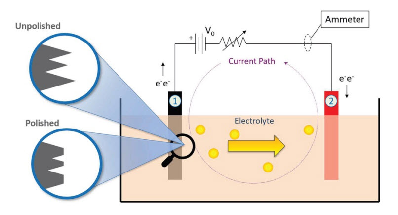
Our highly stable, cost-effective electrodeposition process is ideally suited for use in forming features such as gold bond pads or gold bumps. A subsequent photoresist strip step is followed by the removal of the original gold seed, otherwise known as feature isolation.
This feature isolation step can be performed using dry etch in a vacuum chamber, but that process is expensive and results in a roughened surface of the plated feature. Electrolytic gold deplate is a much lower-cost option that results in minimal CD loss and the smoothest possible gold surface. Further, the process step integrates easily into our advanced and flexible Solstice plating tool when combined with our proprietary Gen4 ECD reactor.
Applications
- Bond pads for microLEDs
- VCSEL p- and n-contact plating
- Gold bump
- BAW and SAW filters
- Air-bridge
- And more…
Features
- Precision wafer rotation, closed-loop flow control
- Voltage-controlled recipe construction
- Continuously filtered chemistry loop
- Optional carbon filtration
- Adjustable diffuser
- Wet-contact plating rotor, customized contact reach
- Levitronix pump with LeviFlow
Benefits
- Extremely uniform removal
- Optimal, responsive removal rate
- Extremely uniform field profile
- Contact reach aligns to existing integration
- Accurate, precise flow rate control
The single-wafer processing Solstice Platform is available with 8, 4, 3 or 2 chambers in customizable configurations, depending on the applications you require.
Technical Data
| Wafer Sizes | 75-200mm (configurable to non-standard sizes, e.g., 160mm) |
| Wafer Thickness | 150μm to >6mm |
| Wafer Materials | Silicon, GaAs, GaN on Si, GaN on Sapphire, Sapphire, Transparent Substrates, and more |
| Flow Rate | 30 lpm |
| Plating Rate | Up to 150μm/minute |
| Within-Wafer Uniformity | <3% (range 2*mean) |
| CD Reduction | <0.2Å on 1200Å seed deplate |
| Roughness | 3Å Ra |
Our highly stable, cost-effective electrodeposition process is ideally suited for use in forming features such as gold bond pads or gold bumps. A subsequent photoresist strip step is followed by the removal of the original gold seed, otherwise known as feature isolation.
This feature isolation step can be performed using dry etch in a vacuum chamber, but that process is expensive and results in a roughened surface of the plated feature. Electrolytic gold deplate is a much lower-cost option that results in minimal CD loss and the smoothest possible gold surface. Further, the process step integrates easily into our advanced and flexible Solstice plating tool when combined with our proprietary Gen4 ECD reactor.
Applications
- Bond pads for microLEDs
- VCSEL p- and n-contact plating
- Gold bump
- BAW and SAW filters
- Air-bridge
- And more…
Features
- Precision wafer rotation, closed-loop flow control
- Voltage-controlled recipe construction
- Continuously filtered chemistry loop
- Optional carbon filtration
- Adjustable diffuser
- Wet-contact plating rotor, customized contact reach
- Levitronix pump with LeviFlow
Benefits
- Extremely uniform removal
- Optimal, responsive removal rate
- Extremely uniform field profile
- Contact reach aligns to existing integration
- Accurate, precise flow rate control
The single-wafer processing Solstice Platform is available with 8, 4, 3 or 2 chambers in customizable configurations, depending on the applications you require.
Let’s Talk
We listen and respond to your unique challenges to provide the right technology at the right time and meet your manufacturing goals. Reach out, and we’ll deliver a solution.


