Indium Bump Plating
Using the Solstice® Gen4 ECD
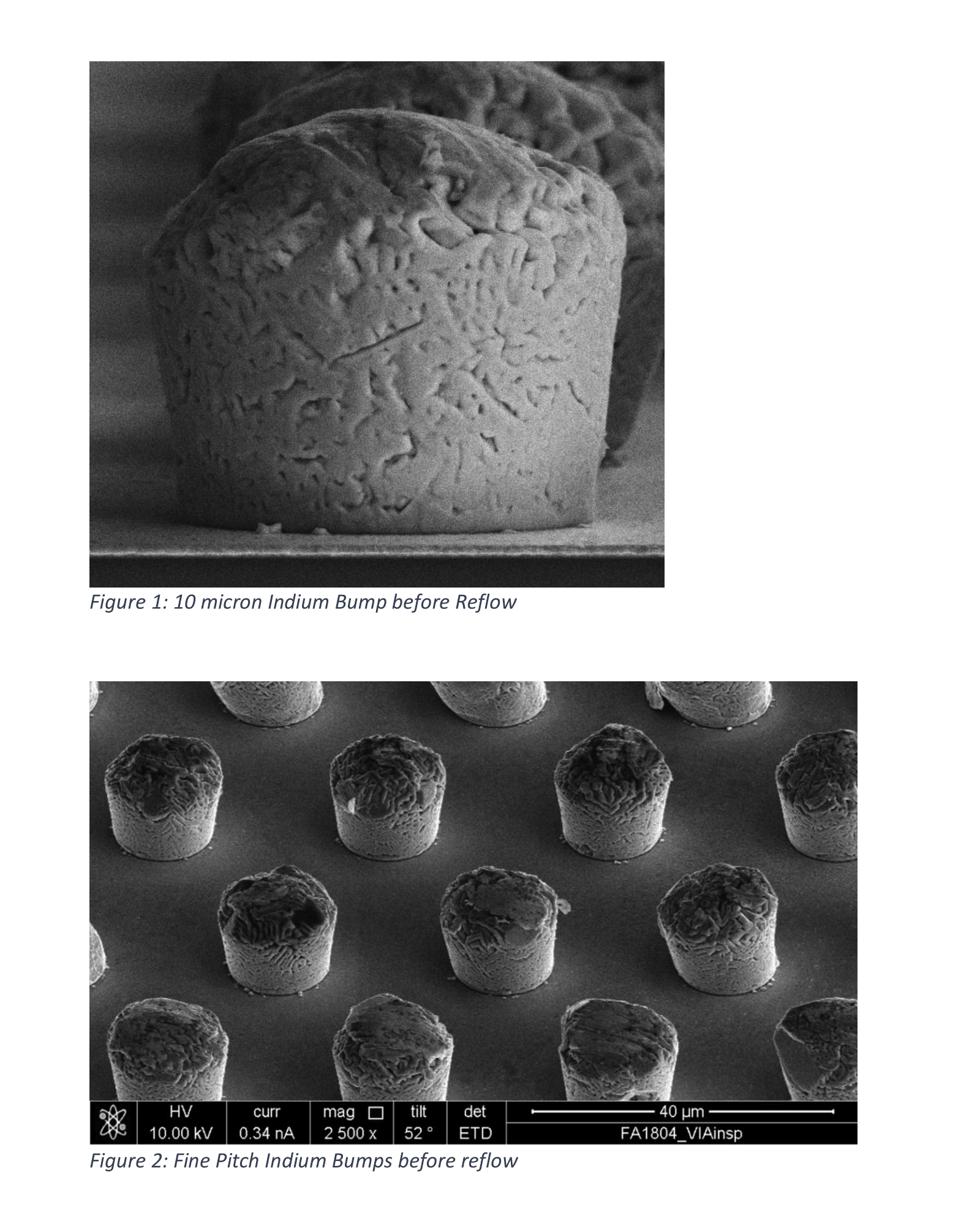
Indium is a unique metal with a low melting point (156°C) and it remains ductile down to absolute zero. For semiconductor devices operating in extreme conditions such as space, Indium is a metal of choice for bonding and packaging. Many companies are turning to electroplated Indium bumps because it is possible to achieve smaller pitches with less waste than traditional evaporation methods.
Our Solstice® Gen4 ECD offers the process flexibility to electroplate Indium to meet all requirements, including precision electric field profile tuning, highly flexible recipe architecture, reactor inert atmosphere, integration of bath monitoring and control, rapid transfer times, and broad platform configurability. A single Solstice Tool can provide Indium Plating, Photoresist strip, and UBM etch (with EPD), for a typical semiconductor flip chip Indium Bump application.
Applications
- Semiconductor Wafer Level Packaging
- Space and Defense
- Sensor Arrays
Benefits
- Small pitches (10 micron)
- High Throughput Manufacturing capable
- Uniform Plating Performance
Learn more about our approach in our article titled “Electroplating innovation enables ultrafine indium bonding“, published in Silicon Semiconductor.
Let’s Talk
We listen and respond to your unique challenges to provide the right technology at the right time and meet your manufacturing goals. Reach out, and we’ll deliver a solution.


