High-Aspect-Ratio Copper TSV Fill Plating
Using the Solstice® CopperMax™ Chamber
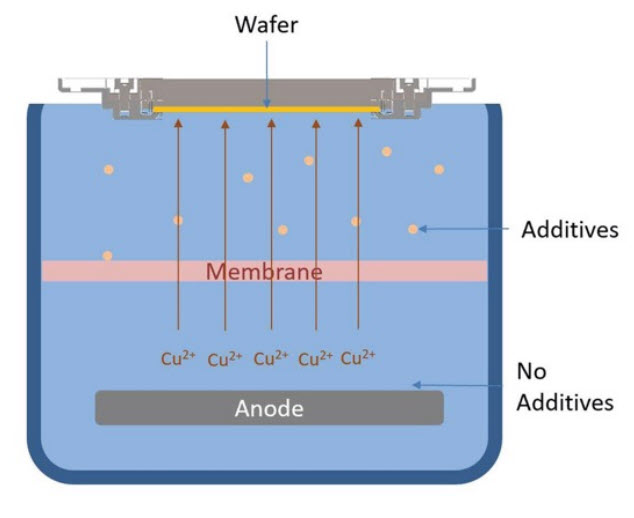
TSV is important to many applications because it provides high bandwidth – high density interconnects. ClassOne Technology has expertise in enabling this process integration flow. Our process experts and partners can help evaluate and inform customers around the critical upstream process integration of Via Etch and Seed Deposition. In addition, ClassOne can provide demonstration and education around the Solstice’s ability to control Electric Field, Fluid Dynamics, and Bath Chemistry. Important to an advanced Copper Plating Chamber is the use of a cationic exchange membrane.
Modern semiconductor copper plating chemistries include expensive, highly engineered organic additives that enable void-free bottom-up fill. These additives, however, are readily destroyed when they come in contact with the copper anode of the plating system. This necessitates ongoing replenishment of additives and significantly increases process costs.
Our proprietary Solstice® CopperMax™ chamber integrates a cationic exchange membrane that separates organic additives from the anode while still allowing high-speed copper cation movement to the wafer. This enables higher plating rates while routinely reducing user chemistry costs by more than 95% – and also delivering excellently plated feature uniformity.
Eliminating Additive Breakdown
The proprietary design of the Solstice CopperMax chamber dramatically reduces the deterioration of organic additives by using a cationic exchange membrane to keep additives from contacting the anode. This significantly reduces chemistry costs while enhancing copper plating quality.
In other chambers, the plating behavior shifts rapidly as additives break down. The bath metrology begins to return inaccurate readings, which leads to erroneous dosing.
Applications
- Wafer-level packaging
- 3D ICs
- Image sensors
- And more…
Features
- Cation exchange membrane to reduce additive use
- Continuously filtered chemistry, optional carbon filtration
- High-precision wafer rotation
- Adjustable diffuser
- Dry-contact, low-maintenance plating rotor
- Customized seal reach
- Levitronix pump with LeviFlow
Benefits
- Additive costs reduced >95%
- Maximized bath life
- Extremely uniform field profile
- Seal reach aligns to existing integration
- Continuously cleaner chemistry
- Precise, consistent flow rate control
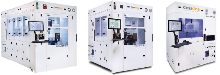
The single-wafer processing Solstice Platform is available with up to 16 chambers in customizable configurations, depending on the applications you require.
Technical Data
| Wafer Materials | Silicon, GaAs, GaN on Si, GaN on Sapphire, Sapphire, Transparent Substrates, and more |
| Flow Rate | 30-60 lpm (dependent on wafer size) |
| Fill Rates | <1 hour for 10×100μm, <20 minute for 5×50μm (dependent on feature) |
| Within-Wafer Uniformity | <5% 3-sigma |
| Wafer-to-Wafer Uniformity | <1% (mean-to-mean) |
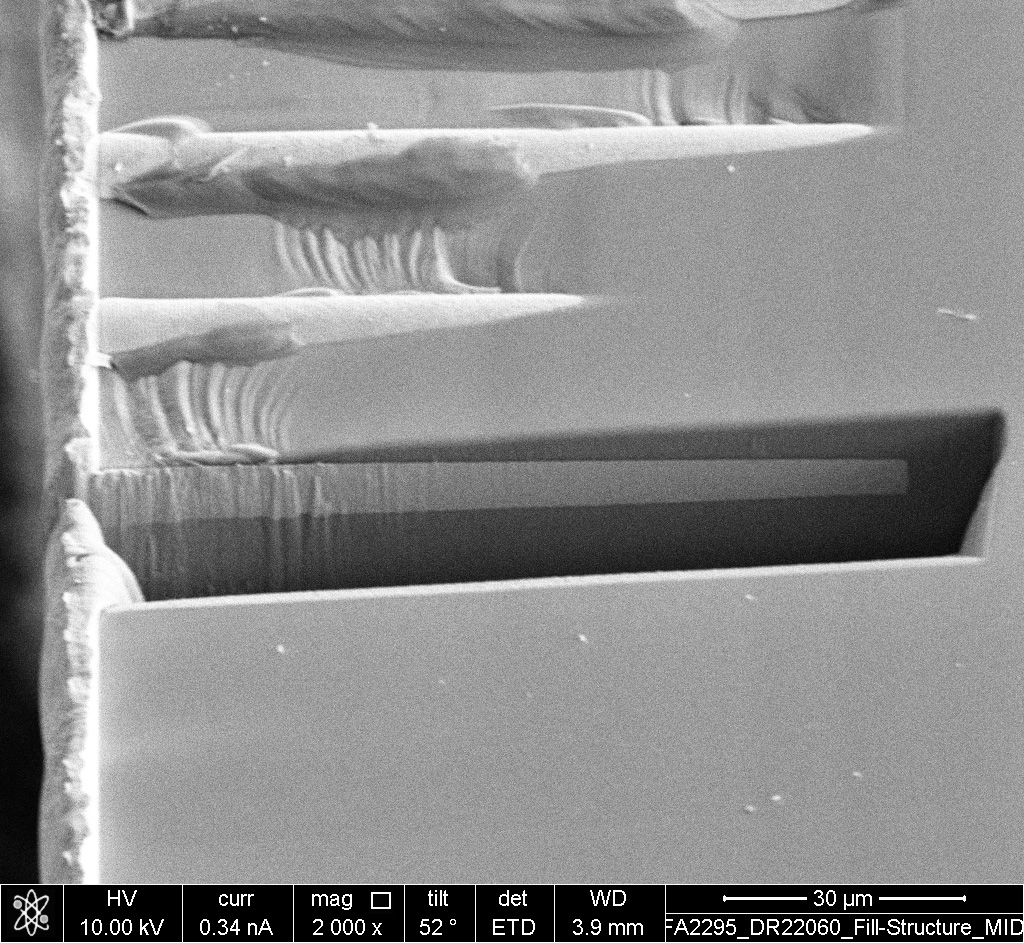
| Fill Quality | Void-free |
| Bath Life | >40 amp-hours per liter (with proper chemistry management) |

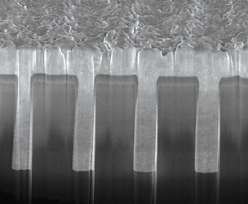
Figure 2: High Aspect Ratio TSV Filled on Solstice CopperMax
TSV is important to many applications because it provides high bandwidth – high density interconnects. ClassOne Technology has expertise in enabling this process integration flow. Our process experts and partners can help evaluate and inform customers around the critical upstream process integration of Via Etch and Seed Deposition. In addition, ClassOne can provide demonstration and education around the Solstice’s ability to control Electric Field, Fluid Dynamics, and Bath Chemistry. Important to an advanced Copper Plating Chamber is the use of a cationic exchange membrane.
Modern semiconductor copper plating chemistries include expensive, highly engineered organic additives that enable void-free bottom-up fill. These additives, however, are readily destroyed when they come in contact with the copper anode of the plating system. This necessitates ongoing replenishment of additives and significantly increases process costs.
Our proprietary Solstice® CopperMax™ chamber integrates a cationic exchange membrane that separates organic additives from the anode while still allowing high-speed copper cation movement to the wafer. This enables higher plating rates while routinely reducing user chemistry costs by more than 95% – and also delivering excellently plated feature uniformity.
Eliminating Additive Breakdown
The proprietary design of the Solstice CopperMax chamber dramatically reduces the deterioration of organic additives by using a cationic exchange membrane to keep additives from contacting the anode. This significantly reduces chemistry costs while enhancing copper plating quality.
In other chambers, the plating behavior shifts rapidly as additives break down. The bath metrology begins to return inaccurate readings, which leads to erroneous dosing.
Applications
- Wafer-level packaging
- 3D ICs
- Image sensors
- And more…
Features
- Cation exchange membrane to reduce additive use
- Continuously filtered chemistry, optional carbon filtration
- High-precision wafer rotation
- Adjustable diffuser
- Dry-contact, low-maintenance plating rotor
- Customized seal reach
- Levitronix pump with LeviFlow
Benefits
- Additive costs reduced >95%
- Maximized bath life
- Extremely uniform field profile
- Seal reach aligns to existing integration
- Continuously cleaner chemistry
- Precise, consistent flow rate control
The single-wafer processing Solstice Platform is available with up to 16 chambers in customizable configurations, depending on the applications you require.
Let’s Talk
We listen and respond to your unique challenges to provide the right technology at the right time and meet your manufacturing goals. Reach out, and we’ll deliver a solution.


