Solder Bump Plating
Using Solstice® CopperMax™ and GoldPro™ Reactors
Solder bump plating is a key process step in advanced packaging, where most functional aspects have already been built on the device. For MEMS and sensors, a chief requirement is to plate features uniformly despite extreme dimensional variation within-wafer and within feature. As a result, management of current density variation is doubly constrained because it directly affects both within-feature thickness uniformity and overall alloy composition. Chemistry and recipe selection, as well as processing chamber design, are therefore critical to achieving high-quality results.
Our Solstice single-wafer platform provides a complete suite of solder bump plating applications with configuration for gold and copper applications as well as novel metals, such as indium. Our proprietary Solstice CopperMax™ reactor enables uniform flow of chemistry against the wafer, uniform current density distribution, and a cationic exchange membrane that protects additives from destruction at the anode. Our Solstice GoldPro™ reactor generates randomized fluid vectors at the diffusion layer of the wafer. This ensures that the diffusion layer is as thin as is practical, and that fluid motion remains directionless. Ultimately, this results in a flat plated feature profile without sacrificing plating rate.
Applications
- MEMS and sensors
- Wafer-level packaging
- More than Moore applications
Features
- Minimal current density variation
- Optimized reactor design for application-specific plating
- Configuration flexibility
Benefits
- Uniform plating of features down to <5µm
- Within-feature thickness uniformity
- Flexible, cost-effective bumping
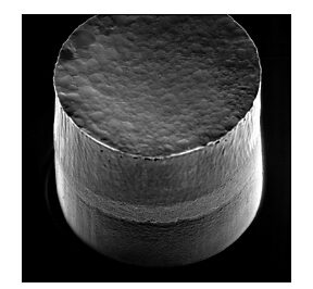
Let’s Talk
We listen and respond to your unique challenges to provide the right technology at the right time and meet your manufacturing goals. Reach out, and we’ll deliver a solution.


