Anodization
Solstice® Wafer Processing
Semiconductor anodization applications have a long-standing history in specialty applications but until now remained highly niche and without mainstream adoption. However, the proliferation of device categories and subcategories which are continually being introduced into semiconductor manufacturing fabs around the world has driven a recent rise in the need for precision formation of anodized films including ultra-high-aspect-ratio pores. Use cases range from invisible reflective coatings for applying discrete coding to microfluidic filtration components to micro-mechanical probe features.
With several key hardware, chemistry and processing considerations, advanced semiconductor plating application can be tuned to highly optimal formation of anodized films.
The typical semiconductor anodization process is characterized by a high potential and low current, meaning the electrolytic cell and substrate combine to form a highly resistive construct. For this reason, avoidance of alternate current paths is key. The electrical contacts connecting the substrate electrically to the circuit must be perfectly protected from even minimal exposure to electrolyte. In other words, a perfect seal to the substrate is a fundamental necessity. Process times tend to be long, >30 minutes and often > 2 hours, and protection of the contacts must be maintained not only throughout a given run but run to run, repeatably. The typical substrate is also brittle, commonly made from alumina, and in some integration schemes can be quite thin. Therefore separation of the substrate from the elastomer in the seal part must account for potential mechanical frailty of the substrate.
Anodization applications tend toward very low processing temperatures, i.e. <5˚C, and tight control to target is critical for perfect pore formation. Closed-loop bath temperature control is critical but not sufficient. Chemistry at the substrate surface can be heated due to the high electrical resistance involved, thus high replenishment of chemistry at the wafer becomes important as well. Direct impingement at high flow rates from a temperature-controlled reservoir ensures no localized warming of chemistry.
The typical electrolyte for anodization is comprised of a dilute organic acid and may or may not include a wet etch step in another commonly available aqueous chemistry. This means that the most economical and lowest cost is achieved with onboard mixing.
The Solstice from ClassOne Technology provides the precision and absolute process control necessary for emerging technologies using semiconductor anodization as a key step in device manufacture and innovation.
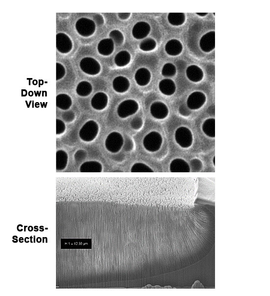
Typical Anodization Performance
- Pore spacing: ±3% of target
- Pore diameter: ±4% of target
- Minimal overlay
- Perfect sealing at substrate edge prevents current leakage
Semiconductor anodization applications have a long-standing history in specialty applications but until now remained highly niche and without mainstream adoption. However, the proliferation of device categories and subcategories which are continually being introduced into semiconductor manufacturing fabs around the world has driven a recent rise in the need for precision formation of anodized films including ultra-high-aspect-ratio pores. Use cases range from invisible reflective coatings for applying discrete coding to microfluidic filtration components to micro-mechanical probe features.
With several key hardware, chemistry and processing considerations, advanced semiconductor plating application can be tuned to highly optimal formation of anodized films.
The typical semiconductor anodization process is characterized by a high potential and low current, meaning the electrolytic cell and substrate combine to form a highly resistive construct. For this reason, avoidance of alternate current paths is key. The electrical contacts connecting the substrate electrically to the circuit must be perfectly protected from even minimal exposure to electrolyte. In other words, a perfect seal to the substrate is a fundamental necessity. Process times tend to be long, >30 minutes and often > 2 hours, and protection of the contacts must be maintained not only throughout a given run but run to run, repeatably. The typical substrate is also brittle, commonly made from alumina, and in some integration schemes can be quite thin. Therefore separation of the substrate from the elastomer in the seal part must account for potential mechanical frailty of the substrate.
Anodization applications tend toward very low processing temperatures, i.e. <5˚C, and tight control to target is critical for perfect pore formation. Closed-loop bath temperature control is critical but not sufficient. Chemistry at the substrate surface can be heated due to the high electrical resistance involved, thus high replenishment of chemistry at the wafer becomes important as well. Direct impingement at high flow rates from a temperature-controlled reservoir ensures no localized warming of chemistry.
The typical electrolyte for anodization is comprised of a dilute organic acid and may or may not include a wet etch step in another commonly available aqueous chemistry. This means that the most economical and lowest cost is achieved with onboard mixing.
The Solstice from ClassOne Technology provides the precision and absolute process control necessary for emerging technologies using semiconductor anodization as a key step in device manufacture and innovation.
Typical Anodization Performance
- Pore spacing: ±3% of target
- Pore diameter: ±4% of target
- Minimal overlay
- Perfect sealing at substrate edge prevents current leakage
Let’s Talk
We listen and respond to your unique challenges to provide the right technology at the right time and meet your manufacturing goals. Reach out, and we’ll deliver a solution.


