Advanced Packaging
Using Solstice® Systems
Wafer Level Packaging (WLP) remains a highly diverse segment in the manufacture of semiconductor devices. Its use extends from cutting-edge, industry-enabling applications such as Fan-Out (FOWLP) for advanced logic to integration of CMOS backplane and discrete device wafers for a vast array of end products. Plating applications range from copper pillar to solder bump to RDL to gold bond pad to TSV fill to hybrid bonding.
Wafers are typically at their most expensive point when WLP begins; this is because all the functional aspects of the device have been manufactured and what remains is integration. Given the diversity of applications (which is present and broad within a given fab – especially foundries), and the cost-sensitive nature of the segment in the manufacturing line, WLP requires broad flexibility and high system reliability. And because this area of fabrication is the primary enabler for More Than Moore and other approaches to cost-effective device innovation, the plating system must be extendible into an unpredictable future too.
Application-specific reactors bring genuine value to the plating applications. This is because integration in WLP may already tightly constrained by heterogeneous metallization and interactions. Therefore copper plating should be fully optimized around the unique requirements of copper plating, and nickel around the requirements for nickel, etc. Gold plating, in particular, tends to be plated in generic systems not specifically designed for its unique characteristics, which include higher sensitivity to fluid dynamics and of course much higher unit process costs.
High throughput and elimination of cross-contamination risks are also key in WLP plating, especially when more delicate applications are included such as high aspect ratio TSV. Plating contacts must perfectly prevent liquid intrusion into the edge exclusion area in order to avoid any number of complications including seed etch and contact plate up. In such case, an elastomeric seal is considered highly important.
At the platform level, because process times in WLP tend to be long, lesser value-added process chambers are best situated to minimize space consumption in the tool so the stacking of prewet and rinse/dry chambers allows space for more plating cells and therefore higher productivity per fab footprint.
The Solstice from ClassOne Technology is ideally suited for diverse requirements such as WLP plating due to its inherent configuration flexibility and its application-specific plating reactors such as the GoldPro and CopperMax.
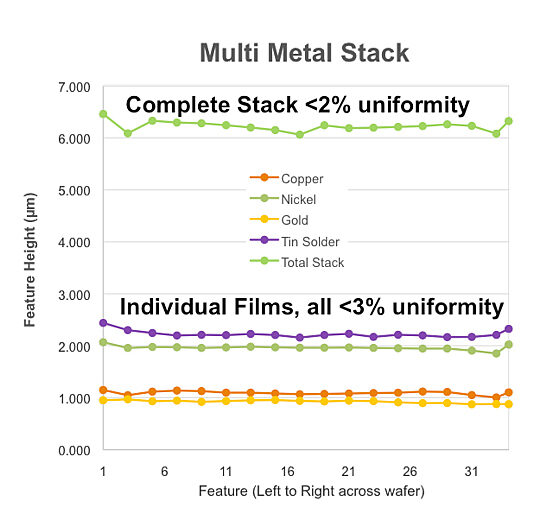
Typical Plating Performance
- Within-wafer uniformity, individual films: <3%
- Within-wafer uniformity, full stack: <2%
- Wafer-to-wafer uniformity: <2%
- Consistently reliable adhesion
Wafer Level Packaging (WLP) remains a highly diverse segment in the manufacture of semiconductor devices. Its use extends from cutting-edge, industry-enabling applications such as Fan-Out (FOWLP) for advanced logic to integration of CMOS backplane and discrete device wafers for a vast array of end products. Plating applications range from copper pillar to solder bump to RDL to gold bond pad to TSV fill to hybrid bonding.
Wafers are typically at their most expensive point when WLP begins; this is because all the functional aspects of the device have been manufactured and what remains is integration. Given the diversity of applications (which is present and broad within a given fab – especially foundries), and the cost-sensitive nature of the segment in the manufacturing line, WLP requires broad flexibility and high system reliability. And because this area of fabrication is the primary enabler for More Than Moore and other approaches to cost-effective device innovation, the plating system must be extendible into an unpredictable future too.
Application-specific reactors bring genuine value to the plating applications. This is because integration in WLP may already tightly constrained by heterogeneous metallization and interactions. Therefore copper plating should be fully optimized around the unique requirements of copper plating, and nickel around the requirements for nickel, etc. Gold plating, in particular, tends to be plated in generic systems not specifically designed for its unique characteristics, which include higher sensitivity to fluid dynamics and of course much higher unit process costs.
High throughput and elimination of cross-contamination risks are also key in WLP plating, especially when more delicate applications are included such as high aspect ratio TSV. Plating contacts must perfectly prevent liquid intrusion into the edge exclusion area in order to avoid any number of complications including seed etch and contact plate up. In such case, an elastomeric seal is considered highly important.
At the platform level, because process times in WLP tend to be long, lesser value-added process chambers are best situated to minimize space consumption in the tool so the stacking of prewet and rinse/dry chambers allows space for more plating cells and therefore higher productivity per fab footprint.
The Solstice from ClassOne Technology is ideally suited for diverse requirements such as WLP plating due to its inherent configuration flexibility and its application-specific plating reactors such as the GoldPro and CopperMax.
Typical Plating Performance
- Within-wafer uniformity, individual films: <3%
- Within-wafer uniformity, full stack: <2%
- Wafer-to-wafer uniformity: <2%
- Consistently reliable adhesion
Let’s Talk
We listen and respond to your unique challenges to provide the right technology at the right time and meet your manufacturing goals. Reach out, and we’ll deliver a solution.


