The Solstice Solution for Advanced Packaging Challenges
Semiconductor wafers are at the most expensive point in the process when packaging begins because all functional aspects of the device have been manufactured – what remains is integration, which poses myriad challenges. Given the diversity of applications within given fabs, especially foundries, and the cost-sensitive nature of the segment, advanced packaging techniques require broad flexibility and high system reliability.
The segment is also seeing significant investment in higher-performing tools that rival front-end-of-line (FEOL) systems in complexity and cost. And because this area of fabrication is the primary enabler for More Than Moore, the plating system must be extendible into an unpredictable future as well. ClassOne Technology’s Solstice single-wafer wet processing platform provides solutions to these challenges. Figure 1 illustrates the platform’s capabilities.
As a leader in advanced packaging solutions, ClassOne leverages the innovative capabilities of its Solstice platform to drive developments in heterogeneous integration such as through-silicon vias (TSVs), through-glass vias (TGVs), hybrid bonding, and interposers for interconnects in 3D chip stacking and wafer-level packaging (WLP). Through collaboration with industry and academia, ClassOne continues to pioneer advancements in process integration, shaping the future of advanced packaging solutions. Let’s look at a breakdown of the capabilities that the Solstice platform brings to the advanced packaging market.
Wafer-Level Packaging
WLP remains a highly diverse segment in the manufacture of semiconductor devices. Its use extends from fan-out (FOWLP) for advanced logic to integration of CMOS backplane and discrete device wafers for a vast array of end products. The Solstice plating system provides a range of capabilities in this area, including:
- Copper pillar
- Solder bump
- Redistribution layer (RDL)
- Gold bond pad
- TSV fill
- Hybrid bonding
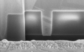
>2:1 aspect ratio

Figure 2: These focused ion beam scanning electron microscope (FIB SEM) images show cross-sectional views of vias and RDL features used in advanced packaging.
Advanced Packaging Applications
Similarly, 3D stacking bonds one chiplet to another while one is still on the wafer – a process known as chip-on-wafer (CoW). Such three-dimensional integrated circuits (ICs) add manufacturing steps, starting with a metal-oxide semiconductor (MOS) circuit and adding 16 or more other ICs interconnected vertically with TSVs to behave as a single device. ClassOne has a standard process of record (POR) for high-aspect ratio vias on its purpose-built plating reactors, utilizing years of process experience and collaboration with all the major chemical suppliers.

Figure 3: Shown here is a SEM of a cross-sectioned fully filled 10:1 aspect ratio
via used for advanced packaging techniques like backside power delivery and chip stacking.
From a lateral perspective, Solstice supports interposer connections, which spread to a wider pitch or reroute connections to different areas. Here, the Solstice platform also has PORs to reliably electroplate the TSV, micro-bumps, and RDL on the top layer of the interposer, which provides horizontal interfacial connections linking component dies. ClassOne’s experience stems not only from traditional silicon devices and compound semiconductors, but extends to glass and other emerging substrate materials as well.
ClassOne’s application-specific reactors bring proven value to plating in advanced packaging integration. Our expertise has yielded an optimized electroplating solution around indium, copper, nickel, gold and other metals and alloys. To complement plating cycle time, the integrated 8-chamber Solstice offers value-added process chambers, including pre-surface cleans, acid etch, or solvent strips, besides vacuum prewet (VPW) and rinse/dry chambers. The Solstice minimizes clean-room space while allowing more plating cells and higher productivity per fab footprint.
The Solstice platform is specially designed for high throughput while eliminating cross-contamination risks in delicate applications such as multi-metal pillars and high-aspect-ratio TSVs.
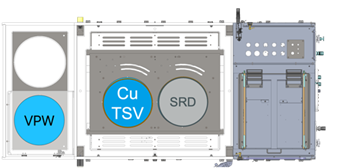
Figure 4:
Solstice LT3, capable of high-aspect-ratio via fill in low-volume fabs; configured with a VPW chamber, copper TSV chamber, and Spin Rinse Dry chamber.
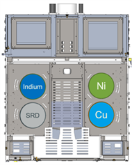
Figure 5:
Solstice S4 configured with a Spin Rinse Dry chamber and copper, nickel, and indium bump plating.
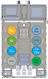
Figure 6:
Solstice S8 configured for multiple processes including multi-metal pillars, copper vias, photoresist strip, and seed etch.
Contact ClassOne Technology to learn more about our diverse process suite,
including TSV/TGV, hybrid bonding, and interposer plating
with the Solstice platform’s inherent flexibility and application-specific plating reactors.


