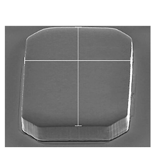
Uniform Nickel Electroplating
Using the Solstice® Gen4 ECD
Nickel electroplating is a critical technology process in semiconductor manufacturing and advanced packaging applications. The predominant challenges during nickel deposition involve intrinsic stress, film passivation and bath maintenance that can lead to significant yield issues. Overall flexibility and design of the plating platform along with specialized nickel electroplating recipes are critical to balance density and plating rates for high-quality results.
Our Solstice® Gen4 ECD offers the process flexibility to deposit nickel to meet all requirements, including wide-range power supply, precision electric field profile tuning, highly flexible recipe architecture, reactor inert atmosphere, rapid transfer times, and broad platform configurability.
Applications
- Wafer-level packaging
- MEMS
- 2.5D/3D ICs
Benefits
- Reduced film stress
- Fast transfer times
- Uniform plating performance
- High throughput

