About Us
About ClassOne
Experts in Advanced Electroplating and Wet Processing
At ClassOne, our mission is to deliver the world’s highest performing and most elegantly designed electroplating and wet processing systems for the manufacture of advanced microelectronics. Engineered for maximum efficiency and flexibility on the manufacturing floor, our systems offer a comprehensive range of electroplating and wet systems solutions validated, tested, fab proven, and designed for top performance in both volume and R&D fab environments
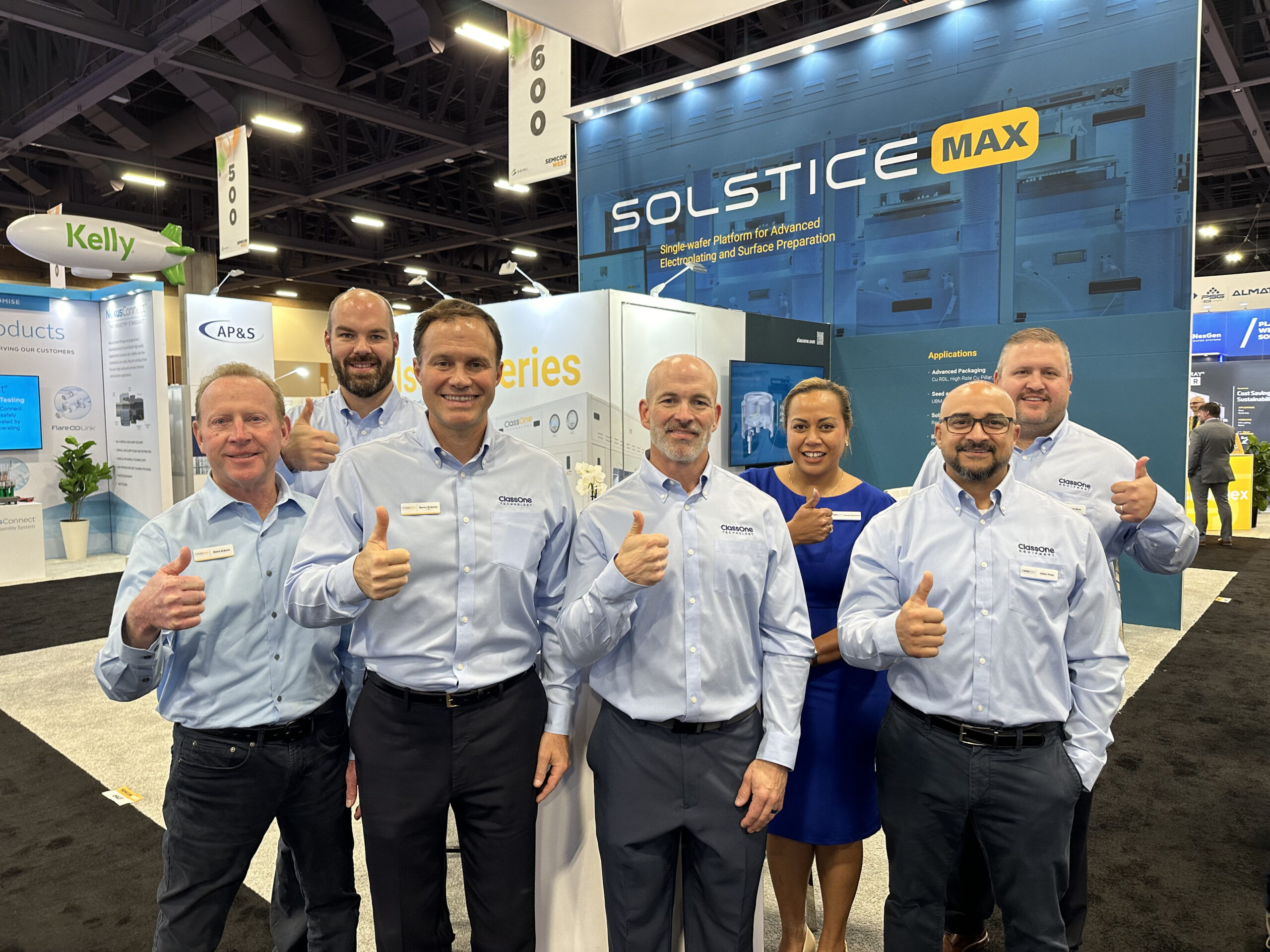
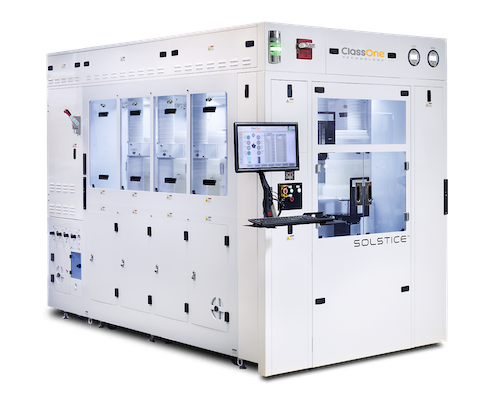
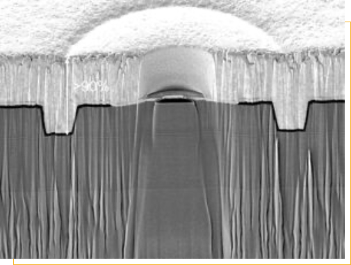
Proven process technology with high-quality results and ROI
Category-leading device manufacturers around the world use our Solstice platform to fabricate devices on a broad array of substrate sizes and materials – from silicon and III-Vs (GaN, GaAs, SiC, InP) to glass, sapphire, and more.
With hundreds of tools installed in advanced production fabs and research organizations worldwide, we provide customized, cost-effective wet processing solutions used to manufacture semiconductor and compound semiconductor devices for the advanced packaging, photonics, artificial intelligence, MEMS and sensors, and RF and power devices markets. Our Solstice® single-wafer platform systems are highly configurable, including both fully and semi-automated systems for electroplating and wet processing applications—with the industry’s most competitive ROI.
Unmatched performance-to-price delivered by world-class experts
Customers select ClassOne tools for their combination of unbeatable performance and lowest total cost of ownership. This is the result of ClassOne’s platform design, elegantly engineered to deliver an unmatched performance-to-cost ratio.
Today, we are working with a majority of the world’s category-leading device manufacturers, including both silicon and compound semiconductor producers of VCSELs, microLEDs, LEDs, laser diodes, MEMS, power semiconductors, RF, photonics, IR sensors, microfluidics, and much more. Our equipment routinely helps fabricate devices on a broad array of substrate sizes and materials..

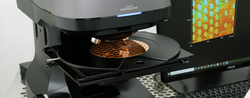
Technology Development Center (TDC)
The TDC provides ClassOne Technology process and equipment experts with a cleanroom environment featuring advanced metrology and process equipment. The TDC affords the capability to process customer wafers, execute process development, and test new products and enhancement to existing products. In addition, customers are always welcome to visit for live technology demonstrations and rigorous technical training. Located near our corporate headquarters in Kalispell, Montana, our world-class Technology Development Center provides our customers with access to the industry’s most advanced tools and a team of experts to solve their unique challenges. From initial conversations through post-installation, we engage with our customers to ensure the highest-quality results.
Our global network
Our vision is to be the partner of choice for those building the devices that enhance the lives of people around the world.
We’ve expanded our global presence via our industry-leading distribution partner and customer service network, establishing an installed base in major fabs and R&D organizations throughout North America, Europe, China, Taiwan, Southeast Asia, Korea, and Japan.

Careers at ClassOne
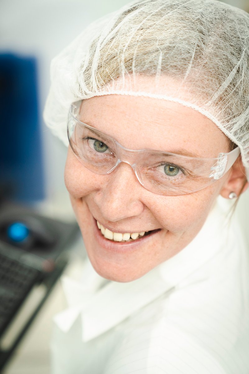
ClassOne Technology is always looking for exceptional team members who share our passion for excellence. If you like the idea of working with a nimble, responsive, high-performance team creating top-quality equipment that stands out and earns respect in the industry… join us at ClassOne Technology.
If you have the qualifications and the drive, please send us your resume: .
ClassOne is an equal opportunity employer offering competitive salaries and comprehensive employee benefits.


