SOLSTICE

Solstice® Single-Wafer Processing Platform
Flexible, Scalable Automated Single-Wafer Processing with Maximum ROI
Our flexible Solstice® S-Series platform offers a broad portfolio of electroplating and surface preparation applications on a single, compact system. Engineered for reliability and uptime, Solstice delivers advanced performance and maximum throughput, while maintaining uniformity. Our team of equipment & process experts integrated reliable, high-integrity, best-in-class components into an elegantly designed family of systems that allow you to realize unparalleled cost efficiency and ROI.
Available with up to 3, 4 or 8 chambers, the Solstice platform can accommodate a variety of substrate types—from traditional silicon devices to compound semiconductors. The systems can reliably and expertly process wafers from 75mm up to 200mm in diameter—whether mounted, thinned, flatted, bowed, or transparent—and can handle multiple wafer sizes on a single system. Wafer rotor changes take less than 20 minutes, minimizing system downtime and contributing to the platform’s ease of operation and maintenance.
Highly Flexible Configurable
Solstice is configurable with process technologies across both electroplating and surface prep, allowing a turnkey solution that meets specific process flow requirements for a wide variety of applications on a single tool.
Common tool configurations:
- Gold electroplating
- Bump and pillar applications – Cu, Ni, & SnAg
- Combo tools – ECD + Seed/Barrier Etch + PR Strip
- Configurations available for R&D, pilot line, and volume manufacturing
Key Applications
Solstice targets six key vital plating and wet surface process applications that encompass a host of capabilities:
- Advanced Packaging
• High-value electroplating and support processes for advanced packaging and other back-end applications such as bumping, pillar, and multi-metal stacks.
• Enabled by high-performance, fountain-style plating chamber design, together with vacuum pre-wet, wet-etch and other wet processing chambers.
- Seed & Barrier Etch
• Fast, uniform application of seed & barrier etch chemistries enabled by the wet-etch chamber with face-up SRD.
• End point detection allows for automatic recipe optimization and ongoing process validation.
- Solvent Processing
• Dedicated or partial solvent tools can be configured with PR strip and metal liftoff (MLO) chambers, using both flood-soak and high-pressure swing arm, enabled by face-down architecture.
• Stainless steel chamber design that is closed and exhausted during process, allows for safe handling and use of solvent chemistries, while minimizing escape of vapors and fumes.
- Back-End Cleans
• Single-wafer solvent, wet-etch and bevel-etch chambers provide the full suite of options for targeted back-end cleans.
• Solstice performs fast, efficient backside and front-side cleans at many steps within back-end processing to ensure wafer and packaging integrity.
- Advanced Gold Plating
• Gold plating is the established standard for many applications, especially VCSEL and RF devices
• The ECD chamber design enables rapid deposition with excellent uniformity across device types.
- Emerging Technologies
• The Solstice platform’s chamber flexibility is ideally suited for developing and scaling new technologies – from glass and microLEDs to hybrid bonding, heterogeneous integration, and more.
Explore By Model
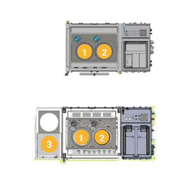
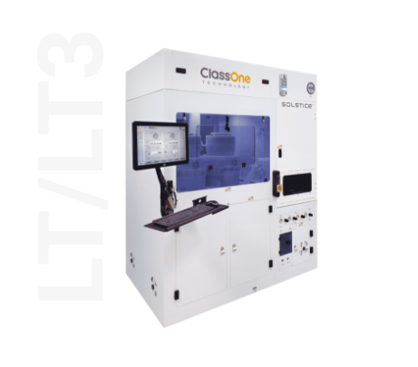
LT/LT3
- Up to 3 chambers: 2 ECD, or 2 ECD plus 1 vacuum prewet chamber
- Economical entry to single-wafer processing
- Easy scale-up path to automated production
- Improved process quality and consistency
- Smallest Solstice system footprint
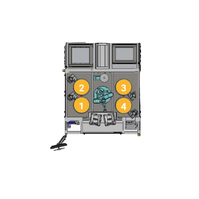
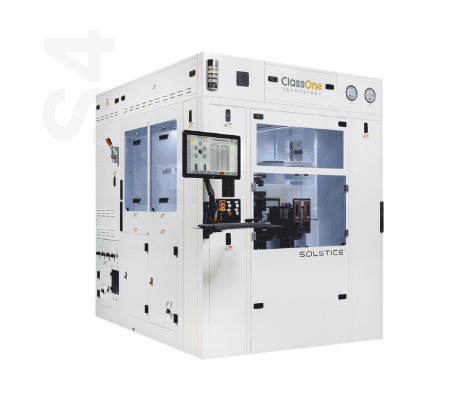
S4
- Includes all the capabilities and performance benefits of S8, but with fewer chambers
- Smaller footprint and lower cost than S8
- Up to 75 wph throughput


S8
- Eight chambers to enable many functions
- Configurable for exceptional plating and surface prep on a single tool, reducing footprint and saving costs
- Handles 75mm to 200mm substrates, including thin or bonded, and transparent or opaque
- High plating rates, excellent throughput, with superior process control and excellent uniformity


